Center for Advanced Materials Engineering

Transforming basic-research into applications to enable technology advancements

Nanotechnology and Smart Materials

The COE-Adv. Mat. Eng. Is conducting several projects in the fields of Nanotechnology and Smart Materials. Besides the evident technological impact, both markets are projected to reach $70.7 Billions by 2027.

Nanoengineered Surfaces for HED targets
Magnetic Nanostructures for Deep Brain Stimulation
Metallic nanorods

Projects

  • Name: Low-Density Materials from Plasma

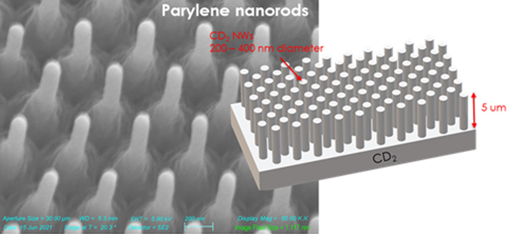
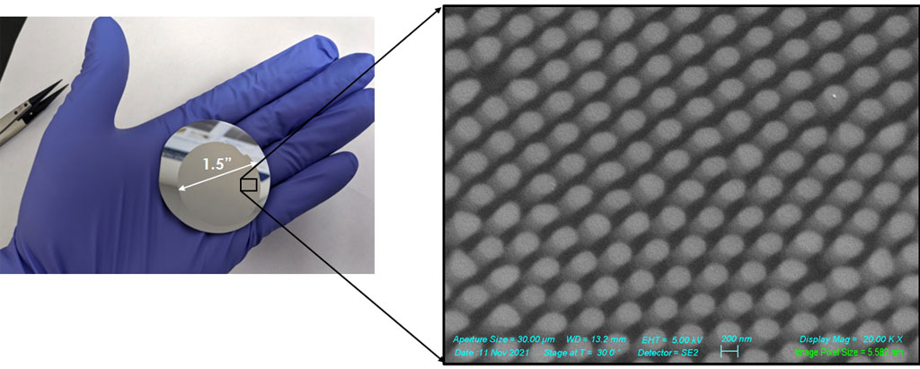
    Our approach to creating novel low density materials, or aerogels from metals is based on the generation of a high pressure metal plasma that is steered towards a substrate that is held in a region of lower pressure. The resulting stream of charged atoms undergoes a phase change forming a narrow beam of nanoparticles. By controlling pressure difference between the two zones as well as the power applied to plasma formation, we are able to control the packing of the nanoparticles as they build up on the substrate. The result is a bulk low density material with features and pore sizes on the nanoscale. This technique has proven to be very useful in creating metal aerogels that are unobtainable by traditional wet chemical methodologies. To date, we have created tungsten, copper, silver and niobium/copper alloys at a fraction of full density without generating one drop of chemical waste. Our attention is now turning towards leveraging these materials in energy storage, water splitting and hydrogen storage applications.

  • Name: W-SiC Graded Films for Plasma-facing Applications

    Tungsten is the leading choice for use as a plasma-facing material within a fusion reactor due to its low erosion and thermal performance. However, several challenges still exist with tungsten that makes it desirable to explore compositionally layered and graded material solutions. One approach is to utilize silicon carbide which has a similar coefficient of thermal expansion to tungsten and is chemically compatible. The benefits of silicon carbide are its excellent thermomechanical properties and neutronics performance. In addition, the permeability of hydrogenic species is extremely low making it an ideal candidate for first-wall and blanket technologies. In this project, we are working on developing the processes for fabricating graded W-SiC materials and will test them within the DIII-D facility located at General Atomics.

  • Name: Nanostructured surfaces for HED, storage

    Our R&D includes the development application of nanotechnology for the fabrication of new targets for fusion and high energy density experiments. These targets present a better coupling with incoming laser energy and therefore produced up to 500X more efficient D-D fusion reactions. 2022 goals are to procure nanostructured targets with customized nanostructures shapes, size, and arrays for mid-rate-rep facilities.

    In the field of smart materials, we’re producing new nanomaterials for applications in biomedical sciences for spinal cord and deep-brain neuro stimulation aimed to pain control, mobility and the treatment of neurological diseases. We’re also interested in the development of sensors, transducers, artificial muscles and electrically activated polymers for industrial, aerospace, and biomedical applications.